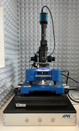
Atomic Force Microscope; Nanowizard 4, JPK/Bruker
The atomic force microscope (AFM) Nanowizard 4 offers multiple application modes to achieve both high resolution imaging and determination of position dependent physical properties, such as electrical conductivity, mechanical stiffness and adhesion forces between tip and surface. To simultaneously measure physical properties and topological appearance of the sample surface, different stages, cantilevers/tips and modes can be chosen. From living cells down to nanoscopic particles and also dynamic changes can be investigated. The variety in samples is just limited by the instrument’s geometry and surface roughness, which should be in the region of interest below 15 µm. By combining different sample stages and measurement modes, structural and surface changes upon different stimuli can be tracked. For instance, the swelling or shrinkage of a material due to external factors such as atmospherical conditions (relative humidity, temperature), or voltage application (actuation).
- Application aim: study of surface topography and mechanical properties
- Mobility: stationary
- Equipment specifics:
- Measurement images up to 100 µm in X & Y and 15 µm in Z height
- Gas and liquid cell (HyperDrive™ fluid imaging for High Resolution AFM).
- Temperature control from 15°C to 60°C
- QI mode (High-resolution quantitative imaging)
- Compatible with Zeiss inverted microscope
- Modes:
- Standard imaging modes: contact mode, tapping mode
- Phase Imaging Mode
- Lateral Force Mode
- Force Spectroscopy (Adhesion, Elasticity and Youngs Modulus)
- Force Modulation
- Kelvin Probe Microscopy (KPFM)
- Conductive AFM (CAFM)
- Nanomanipulation and Nanolithography with special tips
- Sample required: sampling is not needed as long as the studied object can fit in the 20 cm stage and has a thickness no higher than 1.8 cm
- Contact required: surface topography characterization does not require contact, while measuring mechanical properties requires nanoindentations that are however not altering the material surface and structure (indentation depth 5-15 nm).
- Interaction spot dimensions: measurements can be performed in areas that range from 0.5 µm² to 100 µm².
- Application requirements: stable environment with low vibration levels
- Limitations: samples must fit the 20 cm distance between the feet of the device. Maximum thickness is 1.8 cm and roughness (difference between highs and lows) must not exceed 15 µm.
- Average time for measuring: measurement time depends on different factors like mode, resolution or view field. Slowest mode (QI) with maximum view field and high resolution might take up to few hours. Additionally, some time might be invested on finding a suitable area where roughness stays below the limits.
- Average time for processing: image processing might take 5 to 30 minutes depending on the image.
- Output: first output with the whole information is given in .jpk (MB range) but the images can be exported after processing in usual formats such as .png or .tiff, (in the order of hundreds of kB)
- Contacts: Mautra Gallardo, laura.gallardo"AT"tuhh.de
- Location of the equipment: Center for Hybrid Nanostructures (CHyN), DESY, (Notkestraße 85, Hamburg)